

Exynos 2700, the next-generation chip codenamed "Ulysses," is expected to help Samsung make a massive breakthrough in the mobile market in 2027. While the current Exynos 2600 series has already impressed with its copper thermal solution, the latest leaks suggest the South Korean giant has much larger ambitions for its successor, promising to fix all previous weaknesses and deliver peak performance.
SF2P Manufacturing Technology and Next-Generation ARM Core Architecture
A leak from a source that, while not overly famous, is being closely monitored by reputable industry experts, has revealed the broad technical specifications of the Exynos 2700. The first and most predictable highlight is that this chip will utilize Samsung's advanced SF2P manufacturing process. This is the successor, an upgrade from the 2nm GAA (Gate-All-Around) process used in the Exynos 2600. To help readers visualize, GAA is a 3D transistor architecture where the Gate completely surrounds the channel on all four sides, allowing for better electrostatic control and lower operating voltage thresholds, thereby saving more battery life.
The new SF2P process promises to deliver an overall performance increase of approximately 12% and a reduction in power consumption of up to 25% compared to the previous generation SF2 node. Even more notably, this technology allows the prime core to reach clock speeds of up to 4.20GHz, far exceeding the 3.90GHz peak of the Exynos 2600. Regarding core structure, the Exynos 2700 is expected to use ARM Cortex-C2 cores. Note that ARM has changed its naming convention by dropping the "Cortex" label, so these new cores may launch under the names C2-Ultra and C2-Pro. Based on this data, experts predict the Exynos 2700 could achieve an IPC (Instructions Per Cycle) increase of about 35%, with theoretical Geekbench 6 scores reaching 4,800 for single-core and 15,000 for multi-core.
Breakthroughs in Packaging Technology and Thermal Management
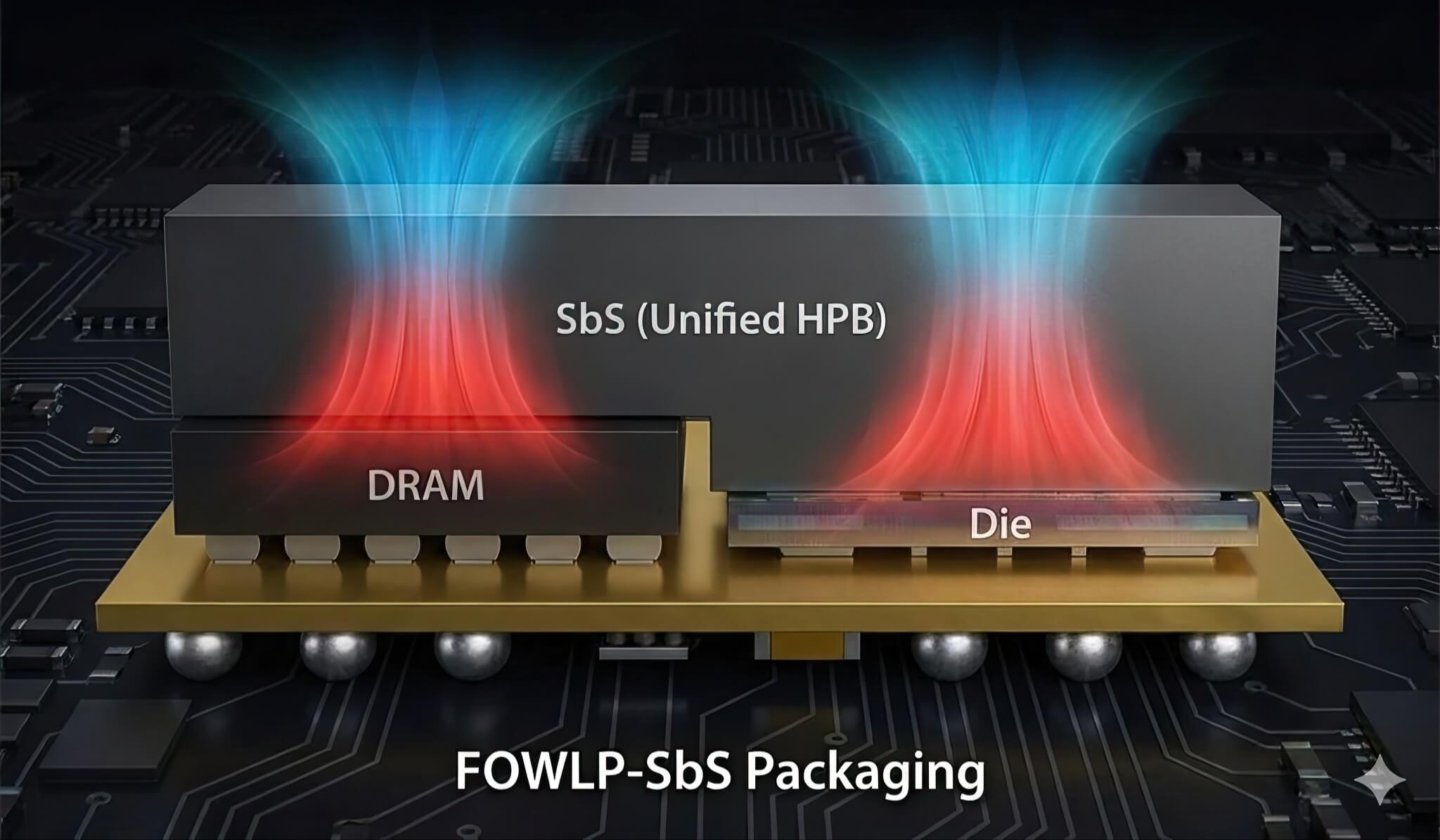
The most revolutionary change in the Exynos 2700 design likely lies in its packaging technology. This chipset is rumored to use FOWLP-SbS (Side-by-Side) packaging technology, utilizing a unified copper Heat Path Block (HPB) for both the DRAM and the Application Processor (AP). This change allows the heat dissipation process to be much more efficient. Unlike the current implementation on the Exynos 2600, where only a portion of the AP is in direct contact with the thermal solution, the new technology on the Exynos 2700 will allow the HPB to cover the entire surface of the processor, ensuring maximum stability during high-intensity operation.
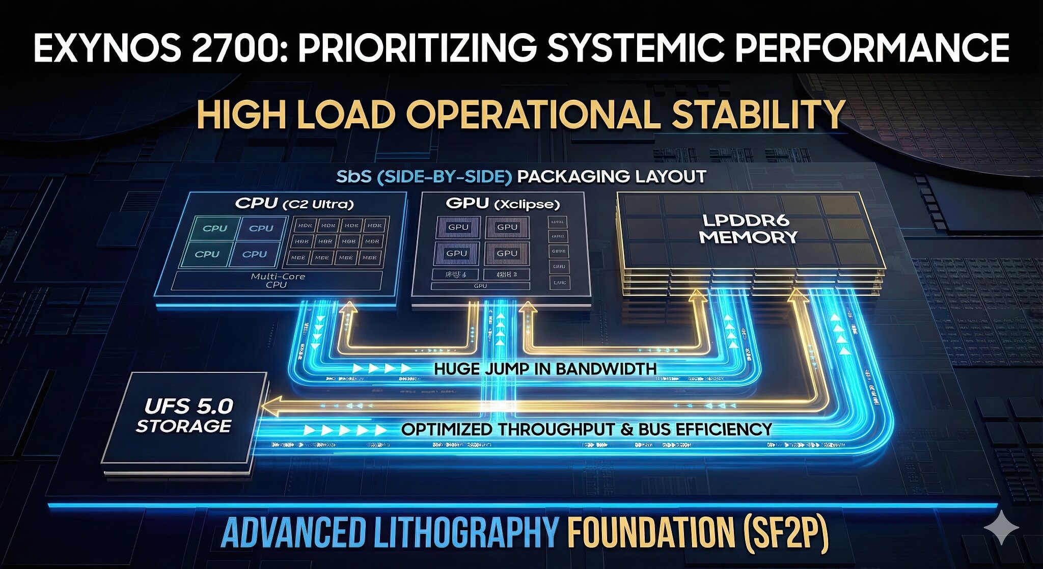
Additionally, Samsung is expected to continue using the Xclipse graphics architecture based on AMD technology for the Exynos 2700. Graphics performance will also benefit greatly from faster data transfer speeds thanks to the support of LPDDR6 memory and UFS 5.0 storage. Overall performance is estimated to increase by 30 to 40 percent. It is worth noting that the LPDDR6 standard supports throughput of up to 14.4 Gbps, an extremely impressive figure.
Uncertainties and Future Expectations for Exynos 2700
Although the leaks are very promising, there are still many unknowns surrounding the Exynos 2700, as the official launch is still many months away. One of the big questions is whether Samsung will choose to integrate the network modem into the chip (integrated modem) or use a discrete modem. A discrete modem is typically less power-efficient but helps simplify the processor manufacturing process, thereby increasing yields.
If all these rumors become reality, the Exynos 2700 (Ulysses) will become a formidable competitor to Qualcomm's next Snapdragon 8 Elite Gen 5. The success of this chip could help the South Korean giant escape its expensive dependence on Qualcomm, opening a new, more self-sufficient chapter for its smartphone business.