
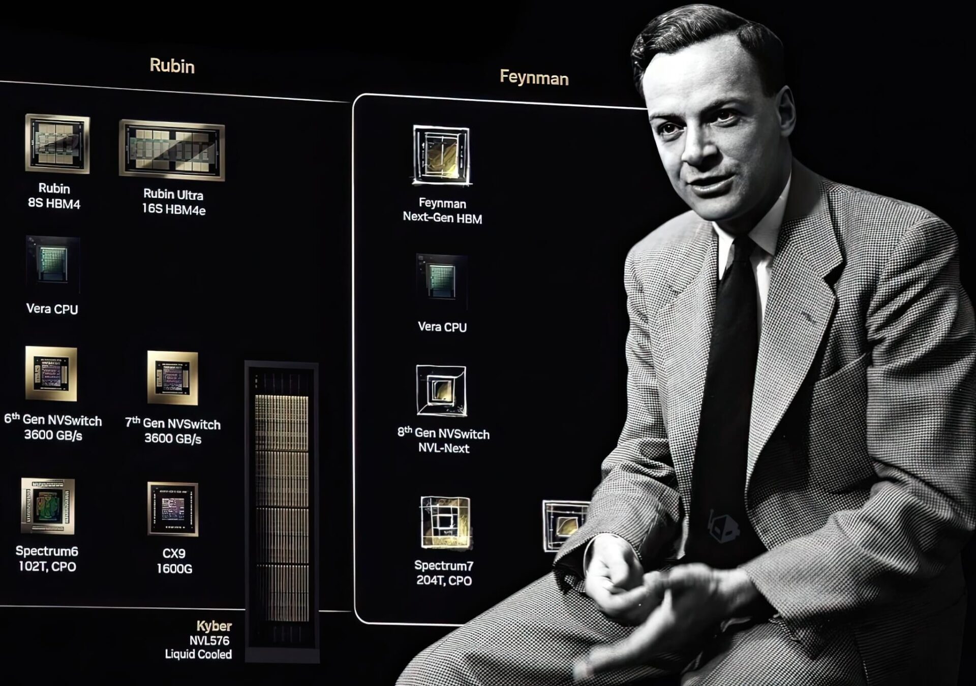
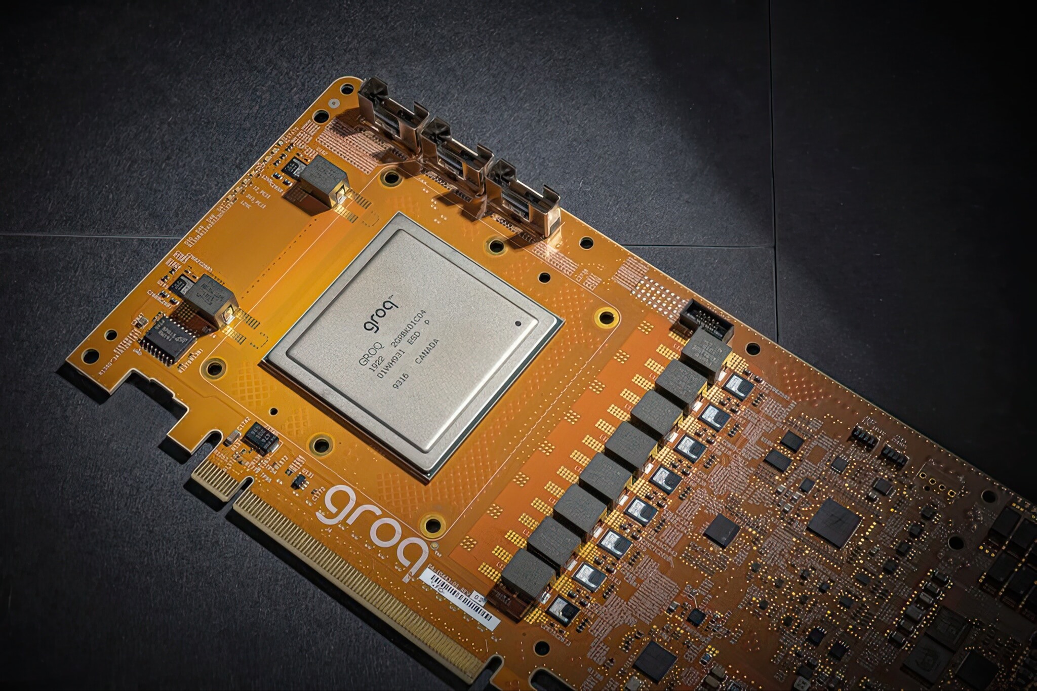
Nvidia is outlining an ambitious plan to completely dominate the AI inference segment with its next-generation Feynman chip series, expected to launch in 2028. According to the latest in-depth analyses, the "Green Team" giant may integrate Groq's Language Processing Units (LPUs) directly into its architecture. Instead of being placed on a single plane, these units are likely to be stacked as separate dies, a method reminiscent of the successful X3D technology utilized by competitor AMD.
Chip Stacking Technology and Nvidia's AI Inference Strategy
The recent intellectual property licensing agreement between Nvidia and Groq regarding LPU units might seem like a modest development if viewed only through the lens of acquisition scale or surface-level revenue figures. However, the reality behind this handshake is Nvidia's massive ambition to lead the AI inference segment through the power of LPUs. The most pressing question for the tech community is how Nvidia will integrate this technology. Based on insights from GPU expert AGF, it appears that LPU units will be stacked on top of next-generation Feynman GPUs using TSMC's hybrid bonding technology.
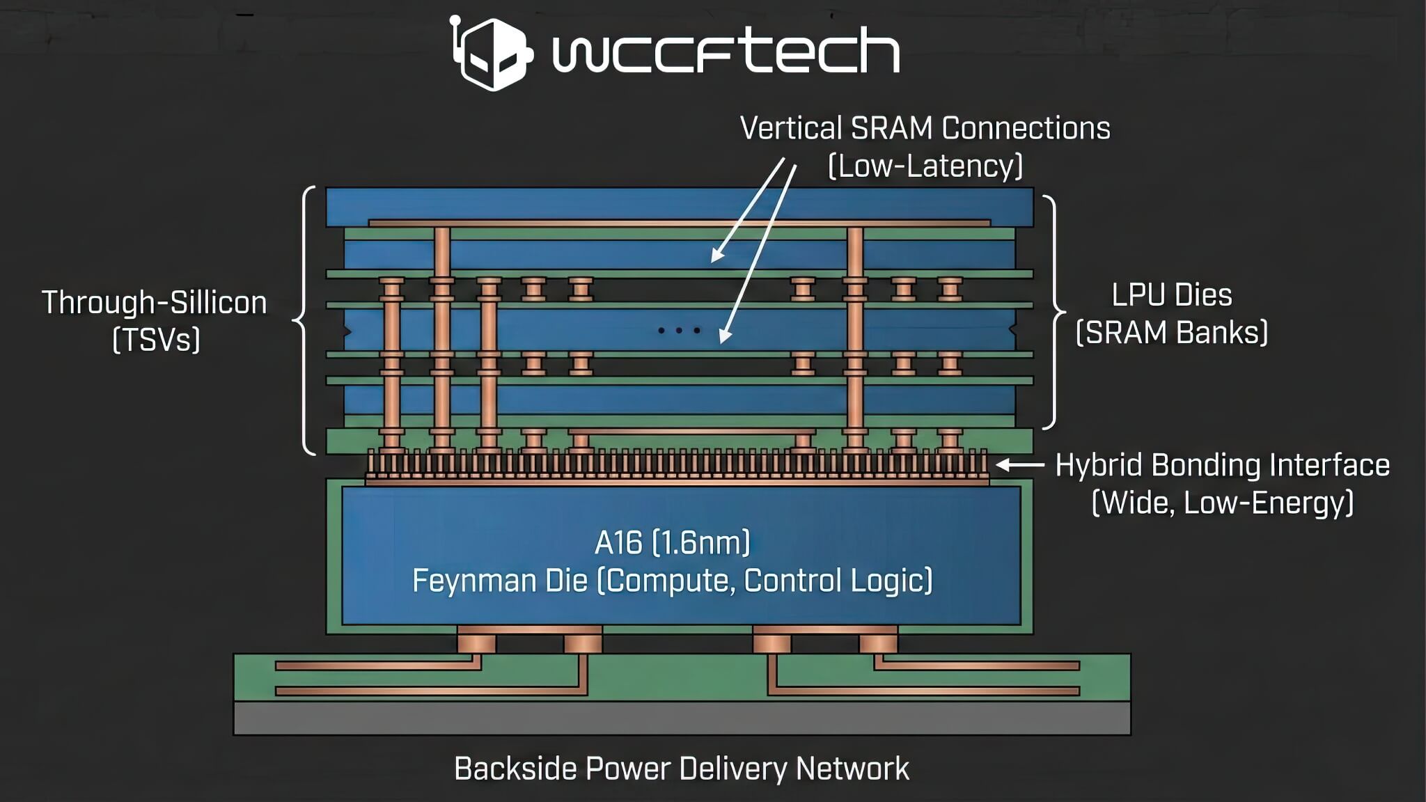
This expert believes that the practical implementation will closely resemble what AMD has done with its X3D CPU lines. Specifically, AMD has utilized TSMC's SoIC hybrid bonding technology to integrate 3D V-Cache memory dies on top of the main compute die. AGF argues that integrating SRAM as a monolithic die alongside the processor might not be the right move for Feynman GPUs. The reason is that SRAM scaling is currently facing physical limits, and attempting to build it on advanced process nodes would lead to high premium silicon area waste, thereby significantly increasing the cost per unit of wafer area.
Instead, a more logical solution is for Nvidia to stack LPU units on top of the Feynman compute die. In this model, chips using the A16 (1.6nm) process will serve as the main Feynman die, containing critical compute blocks such as tensor units and control logic. Meanwhile, separate LPU dies will house large SRAM memory banks. To connect these components, TSMC's hybrid bonding technology will play a pivotal role, allowing for the creation of a wide interconnect interface that consumes much less power than having memory located discretely outside. Furthermore, since the A16 process features backside power delivery, the front side of the chip will be freed up for vertical SRAM connections, ensuring ultra-low latency decoding responses.
Thermal Challenges and CUDA Software Compatibility
While the concept is technically sound and promises high performance, this method also raises several concerns, particularly regarding thermal management. Stacking chip dies on top of each other in a process operating at high computational density is inherently a major thermal challenge. With LPU units focusing on maintaining continuous data throughput, the heat generated could create performance bottlenecks if not managed effectively.
More importantly, the impacts at the software execution level will also increase significantly with this approach. LPU units typically focus on a fixed execution order, which creates a natural conflict between system determinism and flexibility. Even if Nvidia solves the hardware constraints, the primary concern remains how their renowned CUDA software platform will function in an LPU-style execution environment.
This is because LPUs require explicit and specific memory arrangement, whereas CUDA cores are designed toward hardware abstraction to make them easier to program. Integrating SRAM inside AI architectures in this manner will not be an easy task for the "Green Team." It will require a technical feat to ensure the environment combining LPU and GPU is optimally tuned. However, this may be a price Nvidia is willing to pay if they truly intend to lead and dominate the inference segment in the upcoming AI era.