
Building NAND chips using ferroelectric field-effect transistors (FeFETs) could significantly reduce power consumption, according to a new study from the Samsung Advanced Institute of Technology Samsung (SAIT). The company stated they have finally resolved long-standing issues regarding capacity scalability and memory windows, which had undermined previous efforts. Amidst the AI boom driving the construction of massive data centers, the demand for memory is skyrocketing-consequently increasing the already high power consumption of current NAND chips. Samsung researchers are proposing a new architecture that could drastically cut these energy costs. Mobile devices could also benefit if these findings are widely adopted.
FeFETs: Eliminating Pass Voltage and Reducing Power by 96%
Traditionally, NAND chips are scaled by stacking layers on top of each other. The problem is that to fully exploit memory capacity, power must be pushed through these layers sequentially. This voltage (known as Pass Voltage) increases with each added layer, leading to a corresponding rise in total power consumption. Previous attempts to limit power consumption resulted in reduced memory windows. Even other proposals based on ferroelectric materials failed to balance capacity scalability with energy efficiency.
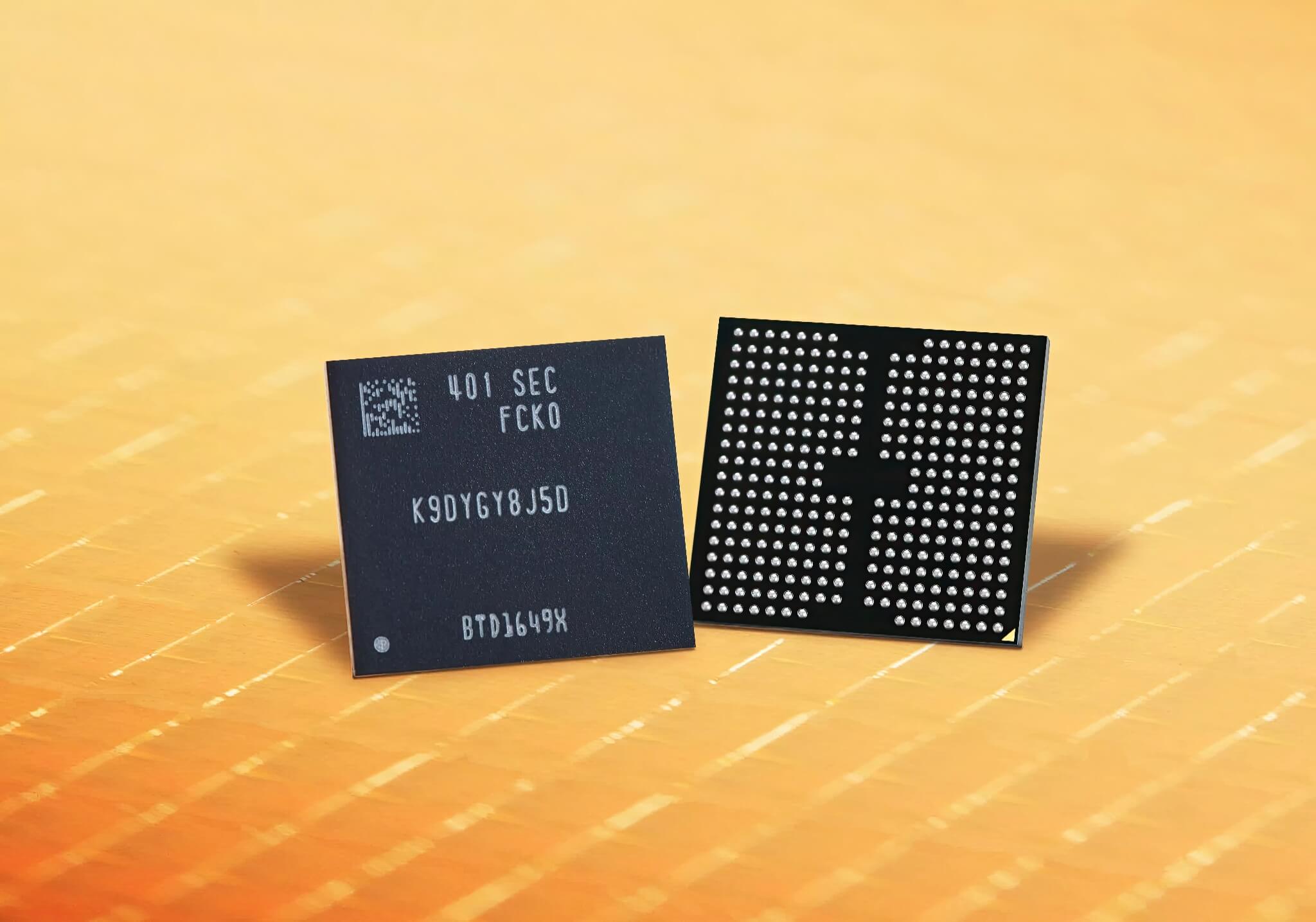
Samsung's approach combines oxide semiconductors with ferroelectric structures to create ferroelectric field-effect transistors (FeFETs), eliminating the aforementioned limitations. FeFETs completely eliminate Pass Voltage, which helps reduce power consumption by up to 96% compared to conventional NAND chips. At the same time, they maintain a multi-level cell density of up to five bits per cell-equivalent to, or better than, today's highest-end memory. Samsung proposes scaling the FeFET design by stacking transistors with 25 nm short channels.
These findings, conducted by over 30 researchers from Samsung's technology institute and semiconductor R&D centers, were recently published in the journal Nature. This work serves as a testament to innovation in materials and memory chip architecture within the semiconductor industry.
Impact on AI and the Future of Battery-less Devices
AI processors and data centers require vast amounts of memory, to the point that they have disrupted the NAND industry, with shortages expected to last at least until 2026. Cutting memory power consumption by nearly 100% could significantly reduce the total energy consumption of AI hardware. The advent of FeFETs promises to address the energy challenges in building massive data centers.
Samsung is not alone in this field. Other companies are also exploring ferroelectric pathways to build non-volatile memory-a type of memory that retains data after power is lost. Whether this approach will prevail over other competitors remains to be seen, but the potential impacts could be enormous for everything from large-scale computing to everyday consumer technologies.
Researchers position this technology as a potential pathway for autonomous, maintenance-free sensor systems that would draw power directly from their environment. This development opens the door for mobile devices that can significantly reduce their dependence on batteries, a major step forward for the consumer electronics industry.