
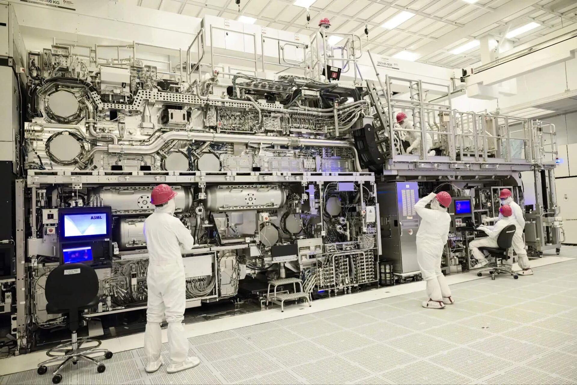
In the fiercely competitive semiconductor technology world, the Dutch corporation ASML Holding holds a central position in the global supply chain, manufacturing nearly all the machines required to create the most advanced integrated circuits. Industry giants like Intel and many other chip manufacturers must rely on ASML's technology to push manufacturing process nodes forward. Recently, Intel officially confirmed the latest results of its strategic partnership with ASML, specifically the successful installation and testing of the TWINSCAN EXE:5200B lithography system. This is considered a key asset in the American giant's effort to reclaim its leadership in chip manufacturing processes and the foundry business.
A major milestone in next-generation chip manufacturing
Intel recently announced significant progress in its collaboration with engineers from the European corporation ASML. The two sides have worked tirelessly together to install, test, and validate their first TWINSCAN EXE:5200B scanner. According to a statement from Intel, this tool will play a central role in the company's massive effort to reclaim its throne in the technology sector, a position they held for decades before facing intense competition from rivals.
This massive and expensive machine has now reached a significant milestone by completing the acceptance testing phase. Technically, the new scanner offers high resolution equivalent to the first generation, the EXE:5000, but the breakthrough lies in its operational throughput. This machine is capable of increasing wafer output to 175 wafers per hour, an impressive figure that helps optimize production costs and time. More importantly, the machine's multi-layer overlay accuracy has been improved to 0.7 nanometers. This milestone is pivotal, signaling that the EXE:5200B is ready to transition from the Research and Development (R&D) phase to mass production, ready to etch new CPU processors and other advanced chip lines.
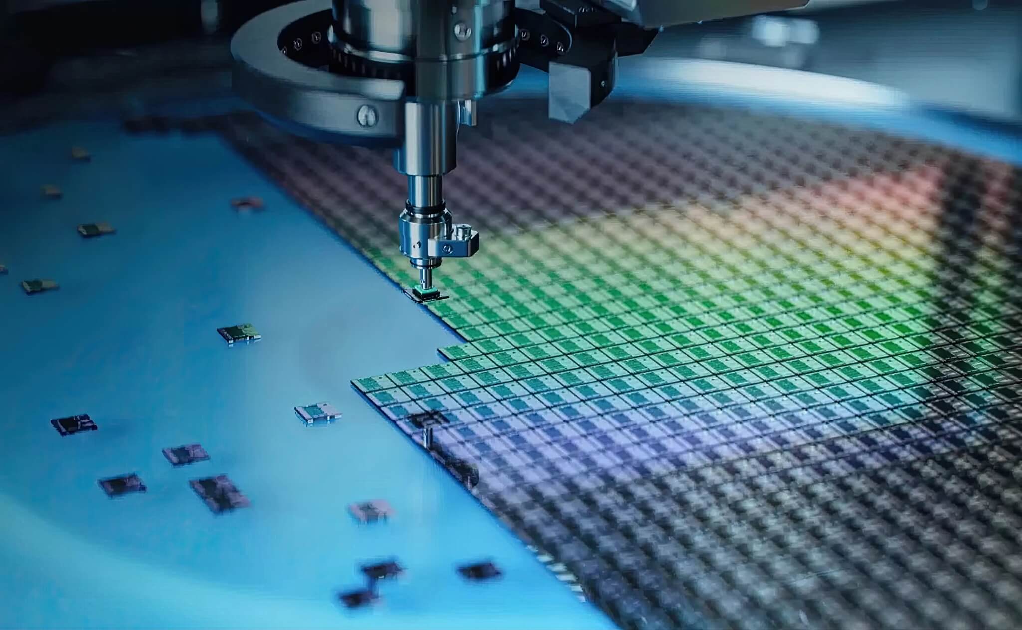
For general readers, overlay accuracy is an extremely important parameter in the lithography-based chip manufacturing process. Imagine stacking tiny Lego blocks on top of each other; even a slight misalignment can ruin the entire structure. With this improved accuracy, Intel will be able to produce chips with even smaller transistors in the coming years. High Numerical Aperture (High NA) Extreme Ultraviolet (EUV) lithography technology is poised to revolutionize chip manufacturing, and in fact, Intel began working with High NA EUV machines at its R&D facility in Oregon in 2023.
Breakthrough improvements in performance and precision
The EXE:5200B version is not merely a minor upgrade; it introduces a series of improvements aimed at enhancing wafer throughput and overall production efficiency. A higher power EUV light source allows for faster wafer exposure at practical doses. Additionally, the wafer storage architecture has been completely redesigned to improve logistics and thermal stability. This significantly enhances performance in complex multi-threading production processes, ensuring the machinery operates as smoothly and with as few errors as possible.
Beyond the efficiency factor, the precision of this scanner positions Intel favorably to push the limits of transistor density in future chip lines. With an overlay accuracy of just 0.7nm, the EXE:5200B machine will help the company manufacture next-generation x86 architecture CPUs and other advanced chip types with smaller transistors, packaged at higher densities. This means our future electronic devices will be more powerful yet more energy-efficient.
Market context and Intel's future vision
However, it should be noted that this state-of-the-art scanner is not exclusive to Intel. SK Hynix, another major chip manufacturer with foundry capabilities, also installed this equipment at its factory in South Korea a few weeks ago. SK Hynix is a company specializing in DRAM and other memory products. This is a sector that analysts predict will be the next victim of an unsustainable AI financial bubble, but the investment in modern machinery shows they are still preparing thoroughly for the future.
While focusing on procuring and validating new production capabilities, Intel has not forgotten its mission to develop its own silicon designs. The company is aiming to move beyond the current RibbonFET gate-all-around architecture toward the new 2DFET model. This architecture is expected to allow the application of damascene-style etching processes in future manufacturing technologies. The combination of the world's best lithography machines from ASML and breakthrough chip designs promises to create an exciting technological race in the near future.