
After much anticipation for the RTX 5000 series, gamers have expressed disappointment following the lukewarm reviews for the RTX 5090 and 5080. So, what about the lower-tier models?
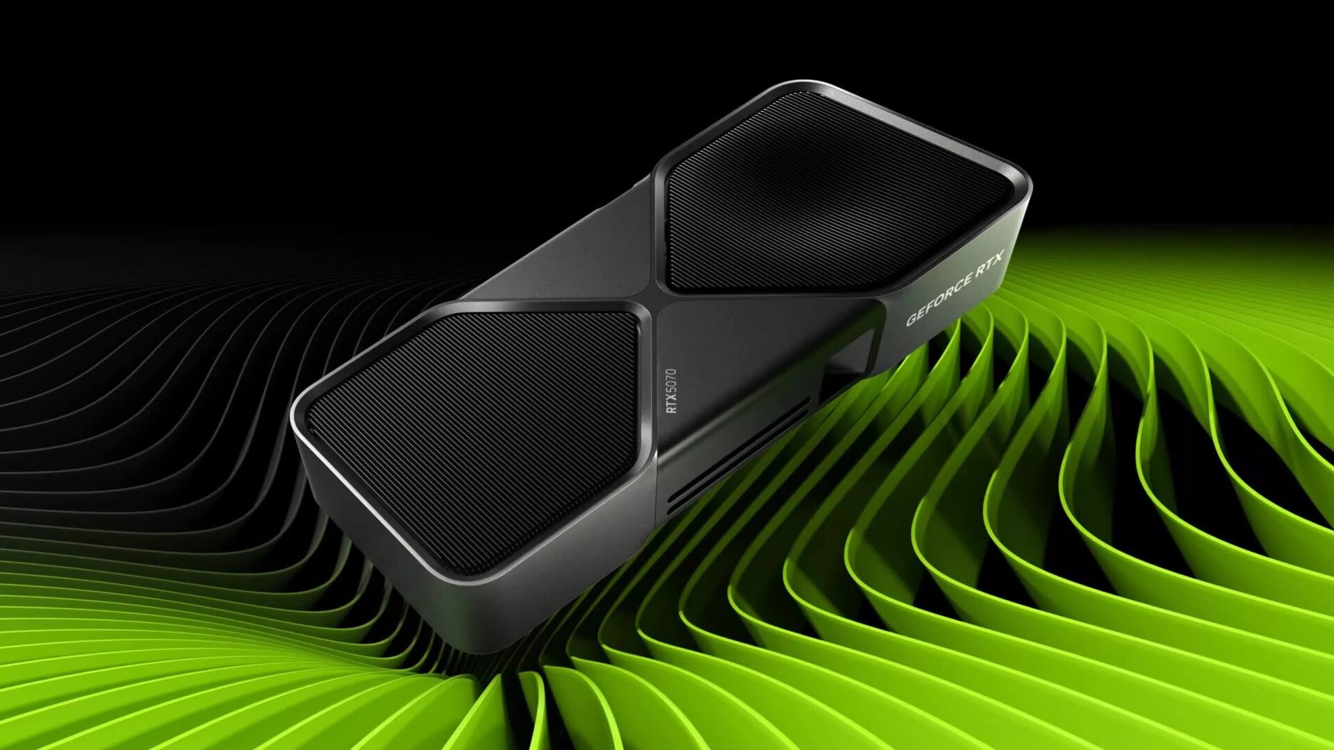
Nvidia has just released the full specifications for the RTX 5070 and 5070 Ti, but it seems the Blackwell architecture has yet to win over consumers.
The RTX 5070 and 5070 Ti were introduced by Nvidia at CES alongside the 5090 and 5080. While key specs had leaked previously, the company has now released official documentation with more hardware details. Starting with the more powerful version - the RTX 5070 Ti, this card uses the GB203 GPU, similar to the RTX 5080. It also features 16GB of GDDR7 VRAM with a 256-bit memory bus, though memory speeds have been reduced from 30 Gbps to 28 Gbps.
The RTX 5070 Ti has a Total Graphics Power (TGP) of 300W, which is 15W higher than the RTX 4070 Ti. The starting price for the card will be 549 USD.
| Graphics Card | RTX 3070 Ti | RTX 4070 Ti | RTX 5070 Ti |
|---|---|---|---|
| GPU Codename | GA104 | AD104 | GB203 |
| GPU Architecture | NVIDIA Ampere | NVIDIA Ada Lovelace | NVIDIA Blackwell |
| GPCs | 6 | 5 | 6 |
| TPCs | 24 | 30 | 35 |
| SMs | 48 | 60 | 70 |
| CUDA Cores / SM | 128 | 128 | 128 |
| CUDA Cores / GPU | 6144 | 7680 | 8960 |
| Tensor Cores / SM | 4 (3rd Gen) | 4 (4th Gen) | 4 (5th Gen) |
| Tensor Cores / GPU | 192 (3rd Gen) | 240 (4th Gen) | 280 (5th Gen) |
| RT Cores | 48 (2nd Gen) | 60 (3rd Gen) | 70 (4th Gen) |
| GPU Boost Clock (MHz) | 1770 | 2610 | 2452 |
| Peak FP32 TFLOPS | 21.7 | 40.1 | 43.9 |
| RT TFLOPS | 42.5 | 92.7 | 133.2 |
| Frame Buffer Memory Size and Type | 8 GB GDDR6X | 12 GB GDDR6X | 16 GB GDDR7 |
| Memory Interface | 256-bit | 192-bit | 256-bit |
| Memory Clock (Data Rate) | 19 Gbps | 21 Gbps | 28 Gbps |
| Memory Bandwidth | 608 GB/sec | 504 GB/sec | 896 GB/sec |
| ROPs | 96 | 80 | 96 |
| Pixel Fill-rate (Gigapixels/sec) | 169.9 | 208.8 | 235.4 |
| Texture Units | 192 | 240 | 280 |
| Texel Fill-rate (Gigatexels/sec) | 339.84 | 626.4 | 686.6 |
| L1 Data Cache/Shared Memory | 6144 KB | 7680 KB | 8960 KB |
| L2 Cache Size | 4096 KB | 49152 KB | 49152 KB |
| Register File Size | 12288 KB | 15360 KB | 17920 KB |
| Video Engines | 1 x NVENC (7th Gen), 1 x NVDEC (5th Gen) | 2 x NVENC (8th Gen), 1 x NVDEC (5th Gen) | 2 x NVENC (9th Gen), 1 x NVDEC (6th Gen) |
| TGP (Total Graphics Power) | 290 W | 285 W | 300 W |
| Transistor Count | 17.4 Billion | 35.8 Billion | 45.6 Billion |
| Die Size | 392.5 mm² | 294.5 mm² | 378 mm² |
| Manufacturing Process | Samsung 8 nm 8N | TSMC 4nm 4N | TSMC 4nm 4N |
| PCI Express Interface | Gen 4 | Gen 4 | Gen 5 |
Nvidia has released performance comparison charts for the graphics cards, comparing them against the RTX 4070 Ti. Unsurprisingly, five out of the six performance benchmarks utilize DLSS.
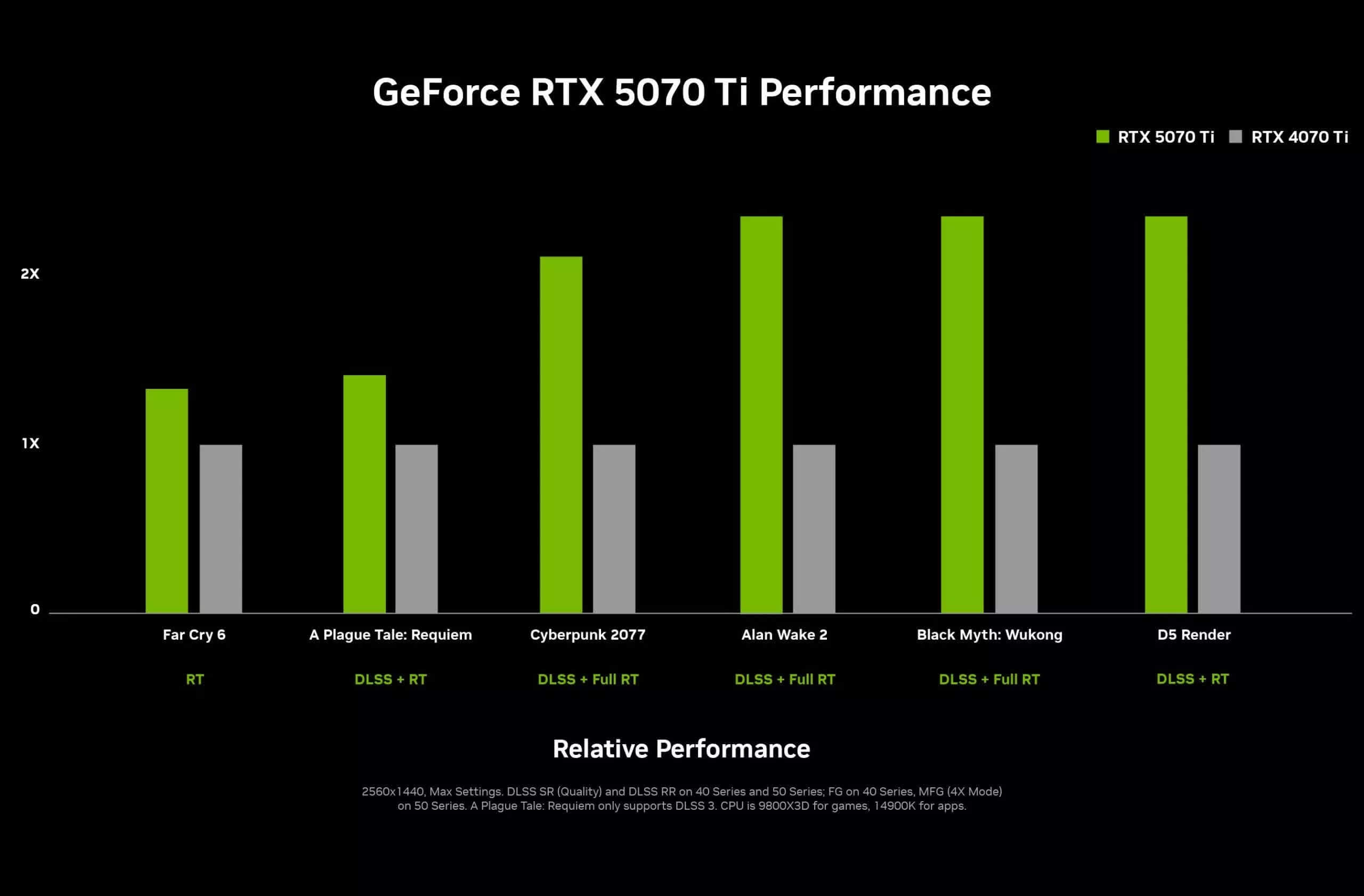
Moving to the RTX 5070 series, it utilizes the GB205 GPU instead of the xx104 chip family used in previous generations. The RTX 5070 features 12GB GDDR7 VRAM (192-bit), similar to the RTX 4070 but with a higher clock speed of 28 Gbps. As a result, memory bandwidth increases from 507 GB/s to 672 GB/s.
The power consumption (TGP) of the RTX 5070 is 250W, which is 50W higher than the previous generation and 30W more than the RTX 4070 Super. The official retail price has not yet been announced.
For reference, at launch, the RTX 4070 Ti was priced at 799 USD, which was 200 USD more expensive than the RTX 4070 (599 USD). This leads many to predict that the RTX 5070 might fall within the 599 - 699 USD price range.
| Graphics Card | RTX 3070 | RTX 4070 | RTX 5070 |
|---|---|---|---|
| GPU Codename | GA104 | AD104 | GB205 |
| GPU Architecture | NVIDIA Ampere | NVIDIA Ada Lovelace | NVIDIA Blackwell |
| GPCs | 6 | 5 | 5 |
| TPCs | 23 | 23 | 24 |
| SMs | 46 | 46 | 48 |
| CUDA Cores / SM | 128 | 128 | 128 |
| CUDA Cores / GPU | 5888 | 5888 | 6144 |
| Tensor Cores / SM | 4 (3rd Gen) | 4 (4th Gen) | 4 (5th Gen) |
| Tensor Cores / GPU | 184 (3rd Gen) | 184 (4th Gen) | 192 (5th Gen) |
| RT Cores | 46 (2nd Gen) | 46 (3rd Gen) | 48 (4th Gen) |
| GPU Boost Clock (MHz) | 1725 | 2475 | 2512 |
| Peak FP32 TFLOPS | 20.3 | 29.1 | 30.9 |
| RT TFLOPS | 39.7 | 67.4 | 93.6 |
| Frame Buffer Memory Size and Type | 8 GB GDDR6 | 12 GB GDDR6X | 12 GB GDDR7 |
| Memory Interface | 256-bit | 192-bit | 192-bit |
| Memory Clock (Data Rate) | 14 Gbps | 21 Gbps | 28 Gbps |
| Memory Bandwidth | 448 GB/sec | 504 GB/sec | 672 GB/sec |
| ROPs | 96 | 64 | 80 |
| Pixel Fill-rate (Gigapixels/sec) | 165.6 | 158.4 | 201 |
| Texture Units | 184 | 184 | 192 |
| Texel Fill-rate (Gigatexels/sec) | 317.4 | 455.4 | 482.3 |
| L1 Data Cache/Shared Memory | 5888 KB | 5888 KB | 6144 KB |
| L2 Cache Size | 4096 KB | 36864 KB | 49152 KB |
| Register File Size | 11776 KB | 11776 KB | 12288 KB |
| Video Engines | 1 x NVENC (7th Gen), 1 x NVDEC (5th Gen) | 1 x NVENC (8th Gen), 1 x NVDEC (5th Gen) | 1 x NVENC (9th Gen), 1 x NVDEC (6th Gen) |
| TGP (Total Graphics Power) | 220 W | 200 W | 250 W |
| Transistor Count | 17.4 Billion | 31.1 Billion | 35.8 Billion |
| Die Size | 392.5 mm² | 294.5 mm² | 263 mm² |
| Manufacturing Process | Samsung 8 nm 8N | TSMC 4nm 4N | TSMC 4nm 4N |
| PCI Express Interface | Gen 4 | Gen 4 | Gen 5 |
This is Nvidia's performance chart for the RTX 5070, compared with the RTX 4070.
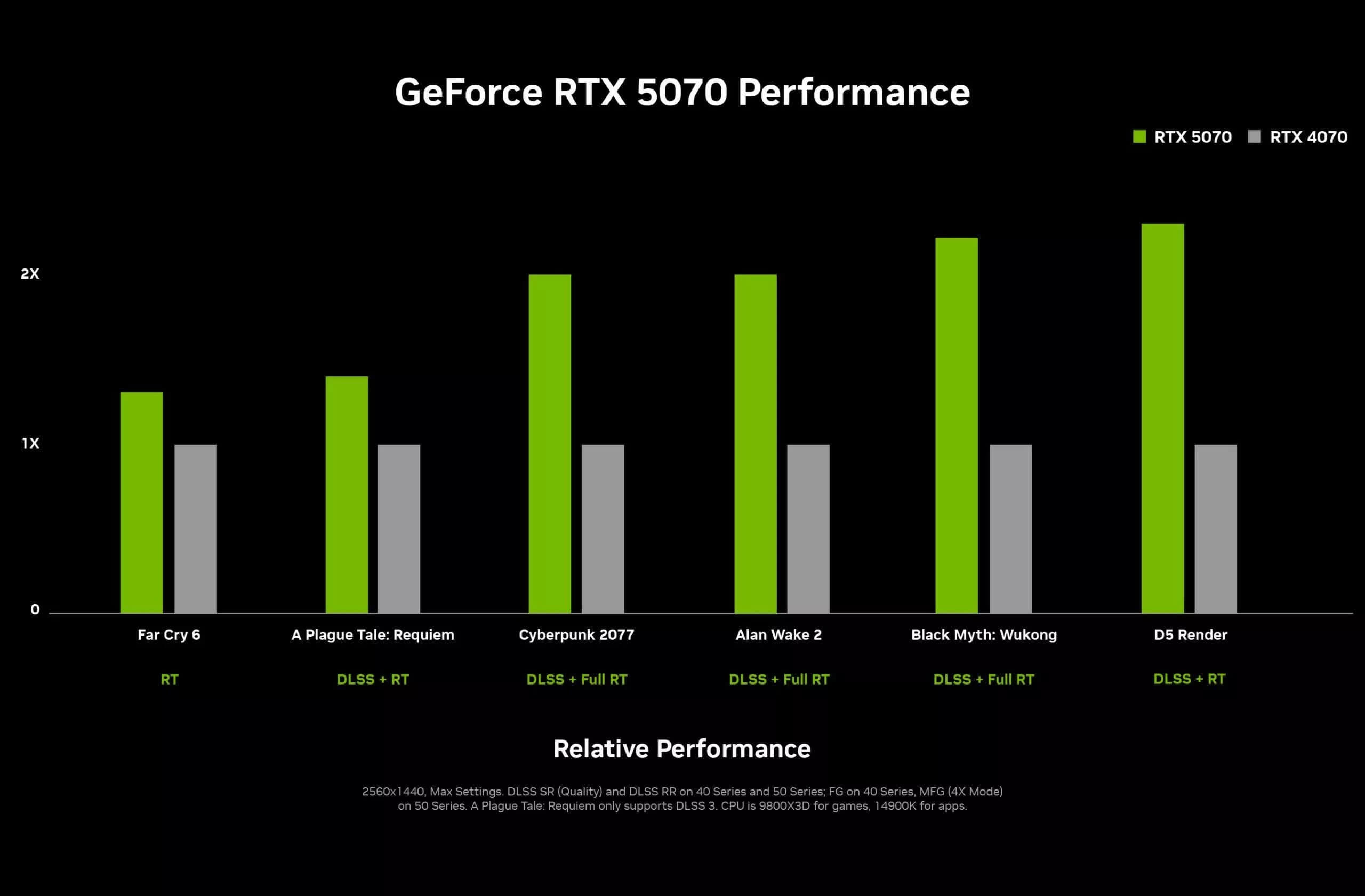
Although Nvidia has not announced an official release date, rumors suggest that the RTX 5070 Ti will launch on February 20th. There is currently no information regarding the release date for the RTX 5070.
Of course, users should wait for reviews before making a decision, but the initial reaction to the specifications of these two cards has not been very positive. In particular, this becomes even clearer following the underwhelming reviews for the RTX 5090 (score 80/100) and RTX 5080 (score 70/100).
The question now is whether AMD can capitalize on consumer indifference toward Blackwell. The company is focusing on more affordable mid-range card models in the Radeon RX 9000 series. The RX 9070 XT, RX 9070, RX 9060, and RX 9050 models are expected to begin going on sale starting in March.